Bicheng Electronics Technology Co., Ltd
Company Profile
Founded in 2003, Shenzhen Bicheng Electronics Technology Co., Ltd is an established high frequency PCB supplier and exporter in
Shenzhen China, severing cellular base station antenna, satellite,
high frequency passive components, microstrip line and band line
circuit, millimeter wave equipment, radar systems, digital radio
frequency antenna and other fields worldwide for 18 years. Our high
frequency PCBs are mainly built on 3 high frequency material
brands: Rogers Corporation, Taconic and Wangling. Dielectric
constant ranges from 2.2 to 10.2 etc.
Bicheng PCB is headquartered in Shenzhen, a city with great
economic vitality. Based in China, we adhere to the philosophy of
servicing small and medium sized companies offering variety of
circuit boards to meet the demands of market.
Main Business & PCB Applications
We maintain the highest standards which support products that
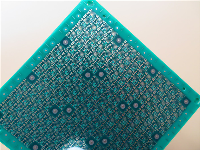
exhibit exceptional quality, performance and reliability. We also have divisions of FR-4 circuit board, flexible circuits
and metal core PCBs featured as prototypes, small runs to mass
production. We actively research and build such high value
added PCB projects as HDI, quick turn, impedance control, heavy
copper and backplane board etc. This has made our PCB products
generate an effective prolongation and complementation, as well as
formation of integrated products line ranging from low-end to
high-end.The circuit boards are used in the industries of home
appliances, portable and consumable electronics, medical filed,
aerospace as well as telecommunications etc.
Main Material Partners


 HDI Low Loss High Temperature PCB for sale")

